Model/Brand/Package
Category/Description
Inventory
Price
Data
-
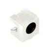
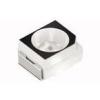
![]() Category: phototransistorDescription: SIDELED® This series of NPN silicon phototransistors that encapsulate OSRAM optoelectronic semiconductors all use SIDELED ® Surface mount (SMD) packaging. The high linearity P-LCC-2 package size is 4.2 x 4.2 x 3.8 mm and is only suitable for reflow soldering of infrared phototransistors, OSRAM Opto Semiconductors4356Get WhatsApp QuoteBOM Quote
Category: phototransistorDescription: SIDELED® This series of NPN silicon phototransistors that encapsulate OSRAM optoelectronic semiconductors all use SIDELED ® Surface mount (SMD) packaging. The high linearity P-LCC-2 package size is 4.2 x 4.2 x 3.8 mm and is only suitable for reflow soldering of infrared phototransistors, OSRAM Opto Semiconductors4356Get WhatsApp QuoteBOM Quote
Scan with WhatsApp to get a quote
-
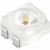
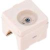
![]() Category: phototransistorDescription: TOPLED® Package # # # phototransistor, OSRAM Opto Semiconductors6022Get WhatsApp QuoteBOM Quote
Category: phototransistorDescription: TOPLED® Package # # # phototransistor, OSRAM Opto Semiconductors6022Get WhatsApp QuoteBOM Quote
Scan with WhatsApp to get a quote
-
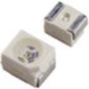
![]() Category: phototransistorDescription: Phototransistor IR Chip Silicon 980nm 2Pin PLCC6922Get WhatsApp QuoteBOM Quote
Category: phototransistorDescription: Phototransistor IR Chip Silicon 980nm 2Pin PLCC6922Get WhatsApp QuoteBOM Quote
Scan with WhatsApp to get a quote
-
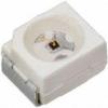
![]() Category: phototransistorDescription: TOPLED® The series of NPN phototransistors packaged with OSRAM Opto Semiconductors adopts TOPLED technology ® Encapsulation. TOPLED ® Phototransistors come in surface mount (SMD) PLCC-2 packages with transparent or daylight diffusing lenses. TOPLED ® Characteristics of phototransistor: High linearity PLCC-2 package surface mount (SMD) half angle: 60 ° Suitable for all soldering methods # # # Infrared phototransistor, OSRAM Opto Semiconductors4076Get WhatsApp QuoteBOM Quote
Category: phototransistorDescription: TOPLED® The series of NPN phototransistors packaged with OSRAM Opto Semiconductors adopts TOPLED technology ® Encapsulation. TOPLED ® Phototransistors come in surface mount (SMD) PLCC-2 packages with transparent or daylight diffusing lenses. TOPLED ® Characteristics of phototransistor: High linearity PLCC-2 package surface mount (SMD) half angle: 60 ° Suitable for all soldering methods # # # Infrared phototransistor, OSRAM Opto Semiconductors4076Get WhatsApp QuoteBOM Quote
Scan with WhatsApp to get a quote
-
![]() Category: phototransistorDescription: OSRAM SFH325-Z Phototransistor SMD7018Get WhatsApp QuoteBOM Quote
Category: phototransistorDescription: OSRAM SFH325-Z Phototransistor SMD7018Get WhatsApp QuoteBOM Quote
Scan with WhatsApp to get a quote
-
![]() Category: phototransistorDescription: Phototransistor SIDELED ® Package size 3.8 x 3.4 x 4.2 mm PLCC-2 is only suitable for IR reflow soldering process # # # phototransistor, OSRAM Opto Semiconductors6930Get WhatsApp QuoteBOM Quote
Category: phototransistorDescription: Phototransistor SIDELED ® Package size 3.8 x 3.4 x 4.2 mm PLCC-2 is only suitable for IR reflow soldering process # # # phototransistor, OSRAM Opto Semiconductors6930Get WhatsApp QuoteBOM Quote
Scan with WhatsApp to get a quote
-
![]() Category: phototransistorDescription: Phototransistor Chip Silicon 980nm 2Pin PLCC2853Get WhatsApp QuoteBOM Quote
Category: phototransistorDescription: Phototransistor Chip Silicon 980nm 2Pin PLCC2853Get WhatsApp QuoteBOM Quote
Scan with WhatsApp to get a quote